In Part 1 I talked about the programming arrangement that I used for the first batch of Z probe boards. After flashing that batch of boards, I got to work on a slightly more automated solution.
My programming process for the first set of boards was like this:
- Place PCB in jig
- Grab programmer
- Position programmer over pins, ensure solid contact
- Press button on PC to commence programming
- Hold programmer in place carefully, wait for programming to complete
- Wait for probe to power up after programming
- Test probe’s trigger distance by hand
I was hoping to remove as many of these steps as I could, so that the process could be simpler and quicker. I decided that the best way to do this was to design a programming jig that incorporated the pogo-pins, so that I didn’t have to do steps 2, 3 and 5.
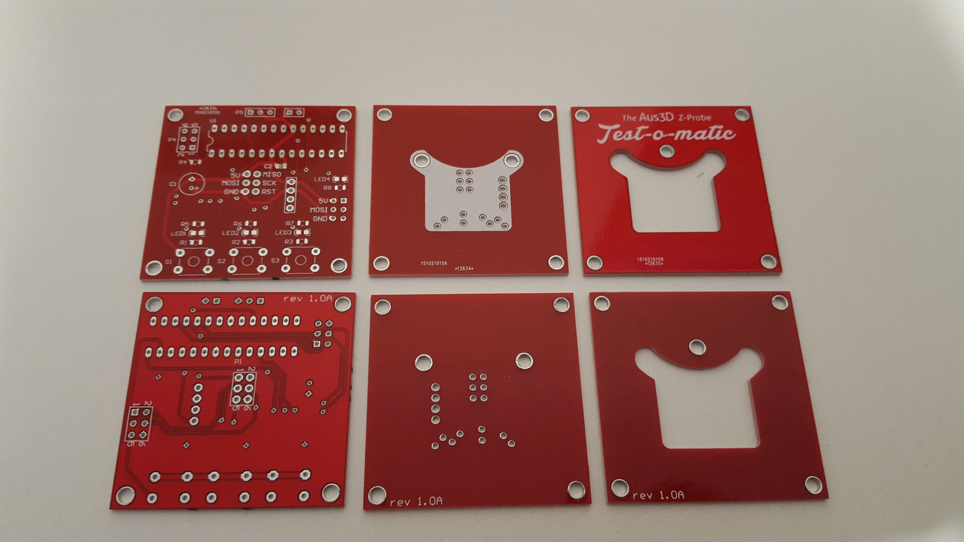
After playing around with it a bit, I settled on a 3-PCB design. I designed the programming jig with two implementations in mind.
Firstly, that the jig would act as an adaptor, with the USB-driven programmer connecting to the jig instead of the hand-held pogo-pin adaptor. This would be relatively easy to implement, as the PCBs only need to connect the pogo-pins to a pin header, and then align everything correctly.
Secondly, that eventually the test jig would operate in a stand-alone fashion, no longer requiring the USB programmer or computer. I included the necessary pads for an ATmega328P and the required supporting components, in the hope that I could later program it to program the Z probes for me.
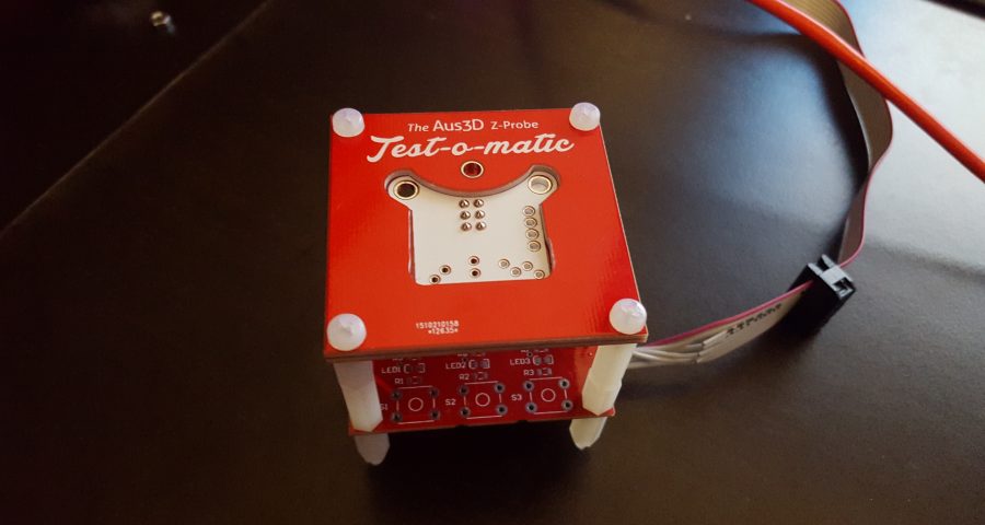
I’m not sure if it’s immediately intuitive how these pieces fit together to make a programming jig, so here’s a photo of the thing assembled.
The bottom PCB has the pin connections for the USB programmer, and is where the pogo-pins are soldered in place.
The middle PCB sits directly beneath the top, and has holes large enough for the pogo-pins to pass through. This PCB keeps the pins in alignment, and acts as a base for the Z probe being programmed to sit on. There is a hole in this PCB corresponding to every through-hole pin on the Z probe, so that it can sit flush and be kept in alignment by these pins.
Finally, the top PCB has a cutout for the Z probe, again to keep things aligned.
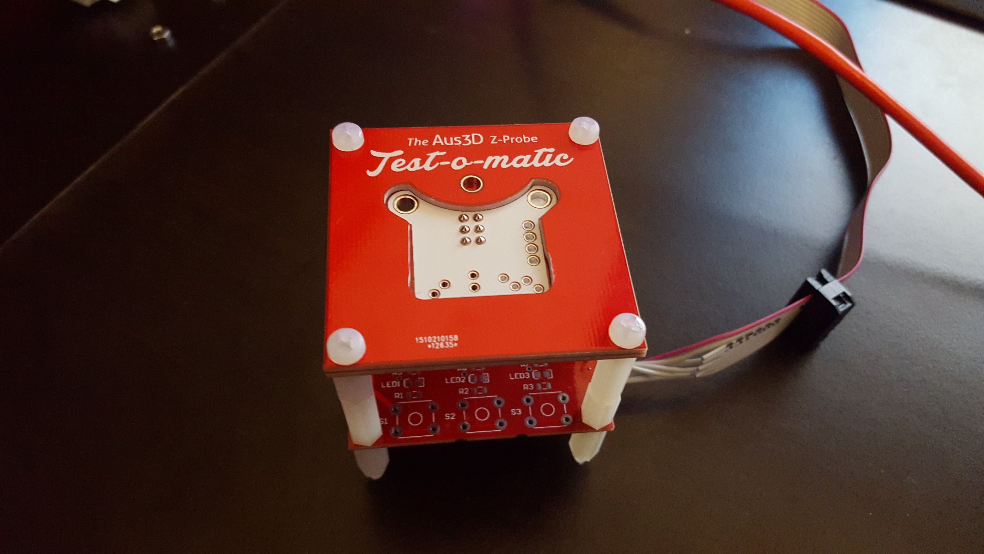
The spacing between the bottom and middle boards is sized so that the pogo pins just protrude through the middle board. Due to their springy nature, when the Z probe that is being programmed is placed on top of them, it has to be pushed down approximately 1mm – far enough to make a solid connection, not so far that there’s any room for the pins to bend or otherwise mess up.
I also included holes for pogo-pins to align with the 4-pin connector used on the Z probe to connect it to the printer control board. The idea behind this was that I wanted to be able to test it as if it was directly connected to the printer, and observe the output signal under test. In practice, the LED indicator provides a suitable indication of when the probe is triggered, and allows for easy testing.
Only a single finger and a little bit of pressure is required to hold the board in alignment during programming. This setup is also much quicker and easier to align, because the Z probe just presses into the cutout and everything is instantly aligned.
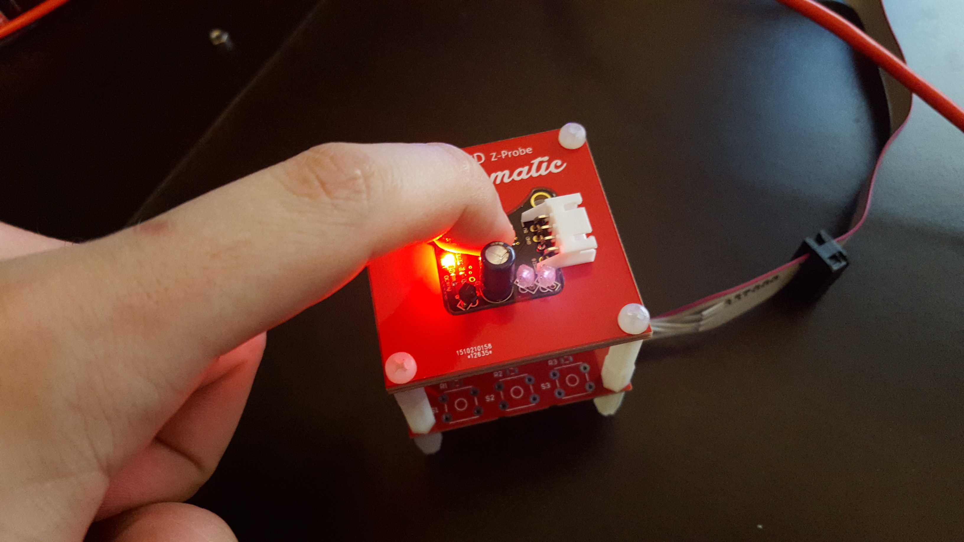
With this setup, I’d removed steps 2 and 3 of programming – as I’d hoped. I still have to hold the probe in place while it’s programmed – I included a bolt hole in the top PCB, thinking I could attach some sort of rotating arm to pin the board in place. Programming only takes a few seconds though, and in honesty it would take more time to swing the arm back and forth than it takes to hold the probe in place.
With this setup, the amount of time to program each board is significantly reduced – I’d go so far as to say the time per board is halved, but I have no data to back that up. I played around with getting the stand-alone programming to work, but to be honest, any extra saving in time beyond this will likely require too much work to be worthwhile – at least at the quantities I’m playing with right now.
Realistically I could probably save another second or two per board if I removed the PC from the loop. It’s also possible that programming from one AVR to another might be slower than from a PC to an AVR – so it’s possible I might not see any speed benefit at all.
I do plan to play around with it in future, but I’m pretty happy with the setup as it is.
I also considered options for automating the test routine. The base PCB includes provisions for connecting a small servo-motor that I intended to use to test the repeatability of the Z probe. So far I’ve just been testing each board by hand, and selecting probes at random for more thorough tests. I’ve not yet had a board fail a repeatability test, so it seems that the current setup is sufficient. Still, it’s something that I might play around with later.
Leave a Reply